
Views: 0 Author: Fenhar Publish Time: 2026-09-30 Origin: Site


Partial discharge in SiC power modules is driven less by operating temperature and more by switching speed. SiC devices switch at 20–100 kV/µs—an order of magnitude faster than IGBTs—forcing voltage across micro-voids and creepage paths before the insulation can relax, which ignites partial discharge. Qualifying insulation to IEC 60270 (PDIV/PDEV) is now mandatory, not optional.
For a power module, insulation is not a passive slab. It is the barrier that stands between a 1200 V silicon-carbide die and a short to the baseplate, and it is asked to survive not only heat but the fastest voltage edges in mainstream power electronics. This guide works the problem from the physics of partial discharge, through the three places it starts inside a module, to a practical qualification checklist you can put on a drawing.
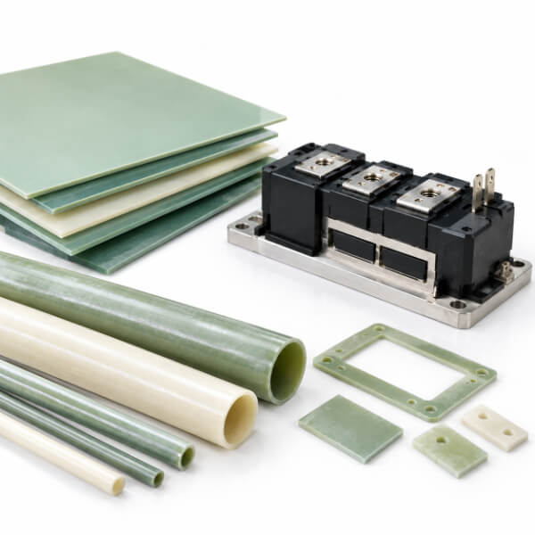
Partial discharge (PD) is defined in IEC 60270 as a localized electrical discharge that only partially bridges the insulation between conductors. The insulation still holds overall—there is no full flashover—but at one small point the local field has exceeded the breakdown strength of a weak spot, and a tiny, repeated spark jumps part of the gap. Each event transfers only picocoulombs of charge and lasts nanoseconds, yet the cumulative effect is what destroys the part.
PD is dangerous precisely because it is partial and progressive. It does not trip a breaker or blow a fuse; it silently erodes. Every discharge injects heat, ultraviolet light, and chemically reactive species into the polymer around it, attacking molecular chains and laying down semi-conductive carbon. Once that carbon track forms, the next discharge finds an easier path, and the process accelerates until a full breakdown bridges the electrodes. NFPA 70B names insulation breakdown as the number-one cause of electrical failures, and partial discharge is its leading early indicator.
There are three families of PD, and a module contains all of them:
Internal discharge — inside a gas-filled void or pore trapped within a solid dielectric. The void has a lower dielectric strength than the surrounding material, so the field concentrates there first.
Surface discharge — along an insulation surface, usually where contamination, moisture, or an inadequate creepage path lets current crawl between electrodes.
Corona / edge discharge — at sharp points, burrs, or the triple point where conductor, insulation, and air meet, where geometry alone concentrates the field.
The short answer is speed. The single parameter that decides whether a fast edge ignites PD is dv/dt—the rate of voltage rise—and SiC operates an order of magnitude beyond the IGBT it replaces.
| Stress parameter | IGBT module (typical) | SiC module (typical) | Why it raises PD risk |
| Switching dv/dt | 5–15 kV/µs | 20–100 kV/µs | Fast edge forces field across voids and interfaces before insulation relaxes |
| Switching frequency | 2–20 kHz | 20–100+ kHz | More transitions per second → more PD events per unit time |
| Waveform | quasi-sinusoidal PWM | sharp unipolar PWM | Unipolar repetition accumulates space charge at interfaces |
| Blocking density | moderate | higher in smaller package | Tighter geometry → higher local field for the same voltage |
| Junction / ambient temperature | up to ~150 °C | up to ~175–200 °C | PD inception is easier at elevated temperature |
The mechanism is not steady-state dielectric strength. When a 20–100 kV/µs edge arrives, the voltage across a void or interface rises faster than the polarization of the material can follow, so the instantaneous field locally overshoots. That transient field enhancement—compounded by capacitive displacement current and rapid charge injection—can push a void into corona even when the peak bus voltage sits below the threshold measured under a slow sine wave. Independent measurements bear this out: under a 60 Hz sine, PD often does not appear until around 7.6 kV, yet the same sample shows continuous discharge when driven by a PWM waveform at roughly 2.7 kV RMS. The peak voltage went down; the dv/dt went up, and that is what lit the discharge.
SiC also changes the accounting. A module in service sees billions of switching cycles, not a one-minute hipot. Each cycle is a fresh opportunity for a micro-discharge, and the damage is cumulative: small events well below a traditional pass/fail threshold, repeating at high frequency, slowly wear the polymer and reshape the local field until a larger discharge becomes inevitable. Repetition rate, not just magnitude, is the aging driver.
Knowing the physics, the next question is architectural: where, physically, does discharge begin? In a modern module there are three recurring locations, and each maps to a different design fix.
Encapsulants exist to protect the die, but any air bubble trapped during potting or gel curing is a ready-made void. The bubble's dielectric strength is a fraction of the epoxy or gel around it, so the field lands there first. This is why void-free encapsulation—vacuum degassing, controlled gel cure, bubble-free dispensing—is not cosmetic; it is PD prevention. A silicone gel that promises to "fill the gaps" only helps if it actually contains no bubbles of its own.
In a direct-bonded-copper (DBC) or active-metal-brazed (AMB) substrate, the ceramic (Al₂O₃ or AlN) is an excellent, intrinsically void-free dielectric—but the bonds and the interface to the baseplate are not. A delamination, a Kirkendall void at a bond line, or a mismatch in permittivity between adjacent layers creates a field concentration at exactly the spot current wants to leak. Interface PD is the hardest to see because it sits beneath the visible surface.
Where a conductor exits the module and runs across an insulating surface—a laminated busbar, a gate-driver PCB, a molded terminal block—the surface becomes a race track for surface discharge, especially once contamination or moisture arrives. This is the domain of creepage and clearance, and of tracking resistance.
This is the single most common qualification gap. The AC dielectric withstand (hipot) test applies a slowly varying sine wave. By construction its dv/dt is low even at high test voltage, so the insulation is evaluated in the regime where PD inception sits highest. A module that is completely quiet on a 50/60 Hz hipot can still develop PD the moment it is switched.
Two effects compound the blind spot. First, parasitic inductance and capacitance in the module, DC link, and gate loop produce overshoot and ringing on every transition, briefly lifting the voltage above the nominal bus and exposing the insulation to a stress the AC qualification never applied. Second, the PWM waveform is unipolar and repetitive, so the field distribution is asymmetric and space charge piles up at interfaces—regions that stayed inactive under AC light up under switching. The conclusion is blunt: a clean hipot is necessary but not sufficient. PD qualification requires a waveform that looks like the one the module actually sees.
IEC 60270, "High-voltage test techniques — Partial discharge measurements," is the measurement backbone. It defines the apparatus—a coupling capacitor and measuring impedance in parallel with the test object, calibrated in picocoulombs—and the parameters that matter:
Apparent charge (q) — the calibrated pC of a discharge event.
PDIV — the voltage on the upward ramp at which discharge first appears.
PDEV — the lower voltage on the downward ramp at which it stops.
Repetition rate (n) and phase-resolved patterns (PRPD) — which reveal where and what kind of discharge is occurring.
The PDIV/PDEV pair is the heart of qualification. PDEV is always below PDIV, and the dangerous case is when PDEV falls under the normal operating voltage: then a discharge that started during a transient keeps running at ordinary voltage and erodes the insulation continuously instead of extinguishing. A margin where PDEV stays above the worst-case operating voltage is the real safety target, not a single pass at one test voltage.
Not every high-voltage test answers the PD question. The table below sorts the common methods by what they actually catch.
| Test method | What it catches | What it misses | When to use it |
| AC dielectric / hipot (IEC 60060, IEC 61800-5-1) | Gross defects, bulk dielectric breakdown, gross voids | dv/dt-triggered PD; small repetitive discharges | Baseline acceptance. Necessary, not sufficient. |
| Impulse / surge withstand (repeated pulses, IEC 60060-1) | Peak withstand, turn-to-turn and layer margin | Fine PD detail; repetition-rate aging | Peak-voltage margin against overshoot/ringing. |
| IEC 60270 PD measurement (AC or PWM excitation) | PDIV, PDEV, apparent charge, PRPD diagnosis | Needs a representative waveform to be meaningful | Core PD qualification. Demand PWM, not just AC. |
| IEC 61934 PD under impulses (repetitive short-rise-time) | PD under switching-like stress; repetition effects | Less standardized acceptance limits across industries | Design qualification for SiC / fast-switching duty. |
For acceptance limits, traction and converter practice gives a concrete anchor: IEC 61287-1 (and EN 61287-1) cites commonly used limits of 10 pC for a component and 50 pC for a system. These are starting points, not absolutes—an application running high dv/dt at altitude or high temperature should tighten them—but they give a specifier a number to write down.
Once the test regime is right, material choice decides the margin. The table ranks the materials a module designer actually has, by their behavior under PD stress.
| Material | PD resistance | CTI (IEC 60112) | Temp class | Typical module role |
| Mica / mica tape | Excellent (inorganic, track-proof) | very high | up to Class H (180 °C)+ | Turn insulation, fire barrier |
| Nomex / aramid paper | Very good | high | Class H (180 °C) | Phase/slot insulation, barriers |
| Polyimide film | Good, thin & high-temp | moderate–high | Class H (180 °C)+ | Gate-driver, control isolation |
| Epoxy glass laminate (FR-4 / G-10 / G-11) | Good if void-free cured | moderate (CTI ~175–225) | Class B–F (130–155 °C) | Busbar insulation, terminal supports |
| Silicone gel / RTV | Fills voids; risky if bubbly | high (self-healing surface) | Class H (180 °C) | Die encapsulation |
| Ceramic substrate (Al₂O₃ / AlN) | Excellent (void-free dielectric) | n/a (inorganic) | very high | DBC / AMB base dielectric |
The table hides the most important rule: PD resistance is a system property, not a material property. A high-CTI laminate laid against a low-CTI film with a sharp permittivity step and a trapped air line will still discharge. Void-free impregnation—ideally vacuum pressure impregnation (VPI)—and clean management of material transitions do more for PD margin than swapping one grade for another. CTI, measured per IEC 60112, then decides how long a surface survives after PD has started: a track-resistant grade buys time before a surface discharge becomes a permanent conductive path.
Most PD is designed in before it is tested in. The cheap fixes are geometric and process-level:
Size creepage and clearance to IEC 60664-1 for the actual pollution degree and overvoltage category, then derate for the SiC transient, not the nominal bus.
Round every edge at conductor exits and grading rings; eliminate triple points where conductor, insulation, and air meet.
Control voids with VPI, vacuum encapsulation, and bubble-free gel—the single highest-leverage process step.
Manage permittivity transitions with stress-equalizing layers instead of abutting materials of very different εᵣ.
Thermal budget: because PD inception falls with temperature, keep the insulation cooler than its class limit where the field is highest.
For a specifier writing the insulation requirement on a SiC power module, the qualification should read something like this:
State the operating voltage and the maximum dv/dt the module will see in service.
Require PDIV above the worst-case switching transient—commonly 1.2× to 1.5× the peak overshoot, measured on a representative PWM or repetitive-impulse waveform per IEC 61934.
Require PDEV above the normal operating voltage, so discharge self-extinguishes when the transient ends.
Set an apparent-charge limit (a starting point: 10 pC component / 50 pC system per IEC 61287-1) and tighten it for altitude or high-temperature duty.
Record a phase-resolved PD pattern, not just a pass/fail number, so the discharge location and type are documented.
Re-qualify on any change to material, mold compound, bond process, or laminate grade—PD is sensitive to exactly those variables.
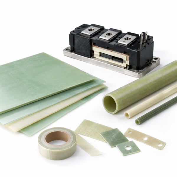
PDIV is the partial discharge inception voltage—the applied voltage at which discharge activity first appears. It is the real dielectric threshold a SiC module meets in service, and that threshold is far lower under the fast, repetitive dv/dt of switching than under the slow 50/60 Hz sine wave used for a hipot. A module can pass a sinusoidal hipot yet have a PWM-PDIV below its own switching transient.
PDIV is the voltage on the upward ramp where discharge starts; PDEV (extinction voltage) is the lower voltage on the downward ramp where it stops. PDEV is always below PDIV. The dangerous case is when PDEV falls under the normal operating voltage: then discharge that started during a transient keeps running at ordinary voltage and erodes insulation continuously instead of self-extinguishing.
No. A 50/60 Hz dielectric withstand test applies a slowly varying sine wave whose dv/dt is inherently low, so it stresses the insulation in a regime where PD inception sits high. SiC switching produces 20–100 kV/µs edges and unipolar, repetitive PWM that triggers PD at much lower peak voltages. A module that is quiet on a hipot can flash over in the field. Hipot is a necessary baseline, not a PD qualification.
Speed. IGBT modules typically transition at 5–15 kV/µs; SiC modules commonly switch at 20–100 kV/µs. That faster edge forces the electric field up across voids, material interfaces, and sharp edges before the insulation can relax, igniting PD even when the peak voltage is below the sinusoidal inception level. Add billions of repetitive switching cycles and higher blocking-voltage density in smaller packages, and the cumulative PD burden on SiC insulation is far heavier.
IEC 60270 is the baseline for partial discharge measurement—apparent charge in picocoulombs, PDIV, PDEV, and phase-resolved patterns—but it is tuned for AC up to about 2000 Hz. For the short-rise-time, repetitive impulses that actually stress a power module, IEC 61934 (electrical measurement of PD under short rise time and repetitive voltage impulses) is the relevant method. A complete qualification uses both: IEC 60270 for the measurement framework and IEC 61934 for the switching-like excitation.
CTI, the comparative tracking index (measured per IEC 60112), is the voltage at which a conductive carbon track forms across a material surface under a contaminating droplet. A high CTI means the surface resists tracking once PD has begun to attack it. For insulation sitting on creepage paths inside a power module, a high-CTI grade (such as track-resistant laminates, mica, or aramid) buys time before a surface discharge turns into a permanent conductive path.
The lesson for anyone specifying insulation around a silicon-carbide module is simple: stop qualifying heat alone and start qualifying speed. The failure that ends a SiC module is at least as likely to be a partial discharge started by a 20–100 kV/µs edge as one started by temperature—and a 50/60 Hz hipot will not see it. Measure PDIV and PDEV on a representative dv/dt waveform, hold PDEV above operating voltage, and treat void-free construction as the foundation of the whole margin.


